

Hi! I am Sai Teja Gorantla, an Electrical Engineering graduate from IIT Kanpur. I interned at Samsung Semiconductor R&D Center, Bangalore (Hardware Profile) in 2017.
As we began the semester with new thoughts and positive energy, came the internship season. Targeting for a core R&D profile, I was both confident and a bit nervous about the internship season.
Preparation
Initially, I was confused whether to opt for coding profile or a core profile. Although I made some initial attempts at coding companies (without any preparation :P), soon I realized that my interests lied in the core field. So I sorted out my priorities and began working in this domain. I brushed up all the courses related to electronics to name a few I revised ESC201 {Electronics Basics}, EE210 {Semiconductor Basics and Analog Electronics} and EE370 {Digital Electronics} courses. I also took a lot of online aptitude tests to improve my accuracy and pace.
Selection Procedure
Samsung came in the very first week of the internship season. No resume shortlisting was there, everyone had to give the test to clear the first round. The test consisted of 60 aptitude questions which were to be solved in 60 minutes with no negative marking. The test was divided into 3 sections: Numerical, Logical Reasoning and English. Each section had 20 questions. You need to have enough practice to solve the questions accurately in the given time. Next came the technical test which was conducted immediately after the aptitude test. We were given a choice to opt either for a coding profile or for a core profile. For the coding profile, 3 questions were asked mainly from trees, linked lists etc. The test for the core profile had around 25 questions ranging from analog electronics, digital electronics, basics of CMOS and few network analysis problems. The test was of 45 minutes with no negative marking. The questions in the technical test were quite tricky. The next round consisted of a GD (inclined more towards technical side) amongst the shortlisted candidates, but this round was skipped and candidates were selected directly based on their resume and performance in the test.
Internship
The most awaited internship began in the mid-May. The weather at Bangalore during this period of time is awesome as compared to much of North India. The electronics core division at Samsung is known as SSIR (Samsung Semiconductor India R&D). The internship began with a fun-filled induction program which was spread over two days. After induction, we were assigned mentors for the projects which were allocated based on our resume and work experience. I was assigned to the CMOS image sensor subdomain in system LSI. Apart from this, there were other domains like Memory Solutions, SOC, FPGA, ASIC, Library IP, Foundry etc. My task was to design CMOS Active Pixel Sensor Noise Model and implement its Noise reduction mechanism known as CDS(Correlated Double Sampling) based on realistic sensor parameters and Pixel Architecture. A major part of the project involved Signal Processing and Semiconductor Physics, luckily I had opted both of them as DE’s before the internship in the sixth semester. Finally, towards the endnote interns’ day was celebrated in which cultural activities were organised and the best projects were presented.
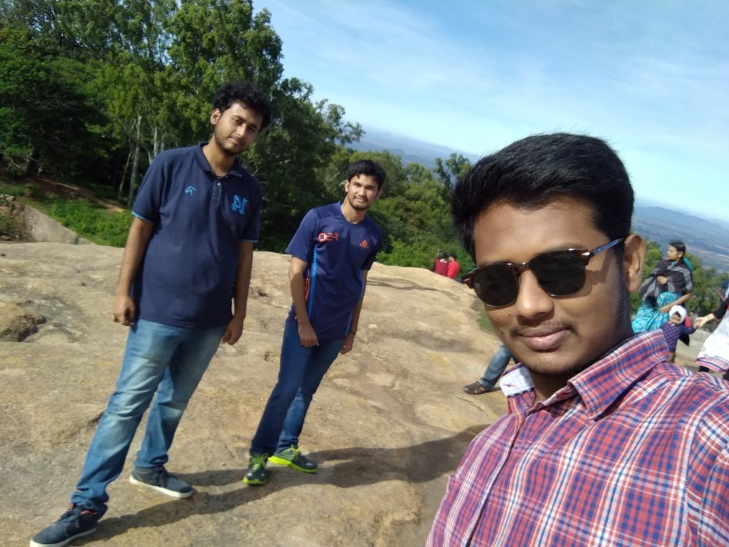
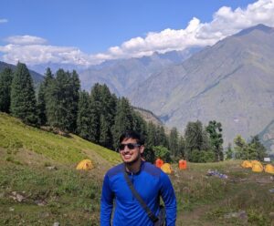
Weekends were exuberant and intriguing. Bangalore has a lot to offer, ranging from amusement parks, malls, historical monuments to adventure sports like trekking and go-karting.
Final Thoughts
The selection process for the Pre-Placement Offer was a bit rigorous. It consisted of mentor’s review of individual performance in the project and mentor’s interview separately. Finally Technical and HR interviews were taken by a panel at the end of second last week. Documentation of the work done during the internship in the last week concluded the internship. I was offered Pre-Placement Offer.
If you are highly inclined towards core field I highly recommend considering this R&D centre. You will be flabbergasted with the hands-on experience of technologies of the real world, which are far beyond breadboards and novice circuits!
In case of any queries, feel free to drop a mail at saiteja@iitk.ac.in
Edited by Smarth Gupta